
1.special note:
You will found the specifications of specific model and related test reports in download center.
2.Our clients:
1、Shenzhen Chongda multilayer circuit board Co., Ltd. 2、Shenzhen Jing Wang Electronic Co., Ltd. 3、Jinxiang Electronics Co., Ltd. 4、Chuanyi computer (Chongqing) Co., Ltd. 5、Tianjin PRINTRONICS circuit Co., Ltd.
3.Application areas:
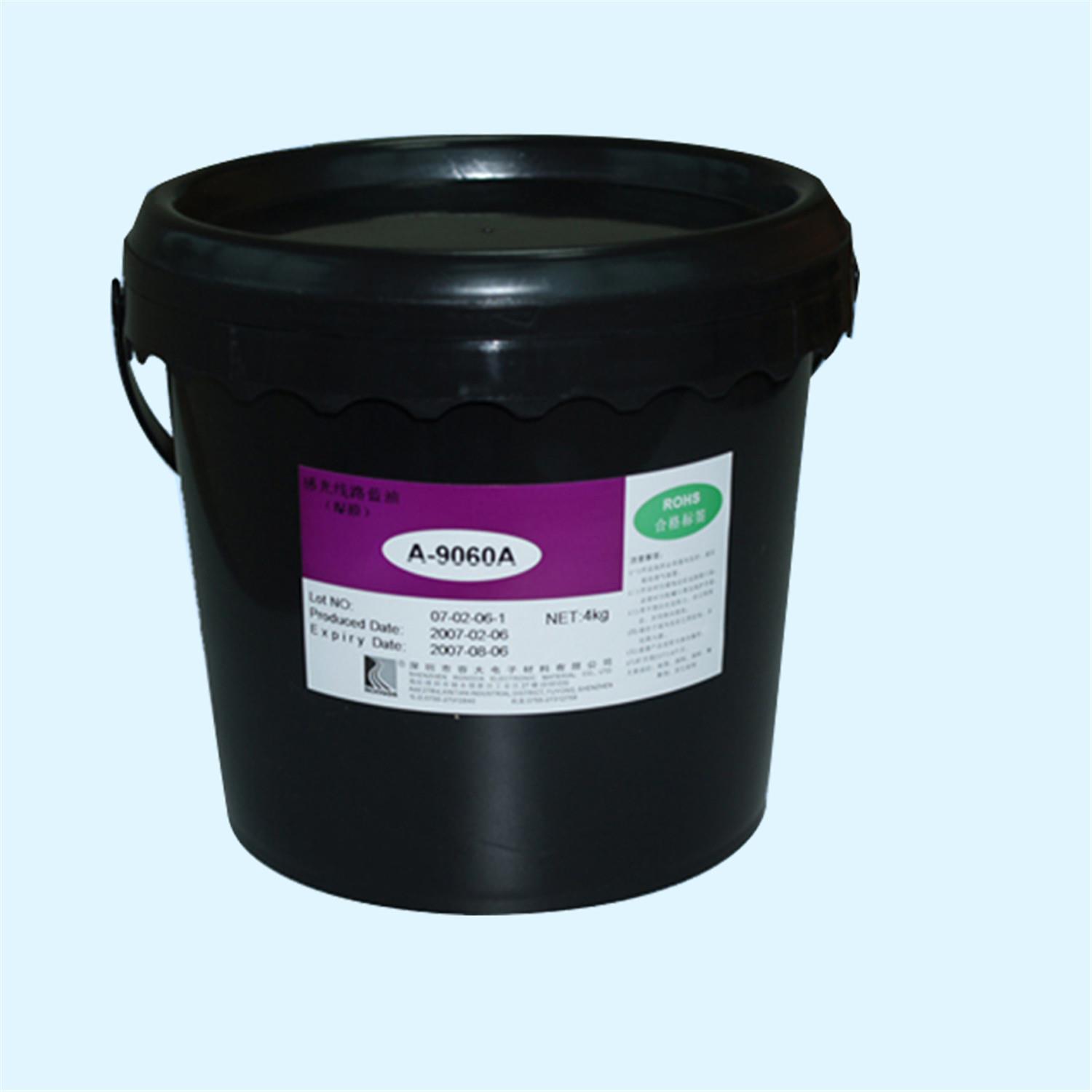
Liquid Photoimageable Solder Resist Ink will form a permanent protection film, not onlythis film can prevent the copper PCB surface fromoxidating, water corroding, solvent corroding and external abrading.But also it can improve electrical insulating properties between lines, even forfull plate surface, so as to prolong the service lifeof the printed circuit board.
Screen printing is the main film-forming way of liquid photoimageable solder resist ink.When the ink is covered to the etching substrate. There will be created a new coating ofcrosslinking curing polymer on the surface of the printing plate after a series of technological process, such as pre cure, exposure, development and post curingetc.Solder resist film has a high light brightness, hardness and adhesion, excellent heat shock resistance, acid and alkali resistance, and solvent resistance properties.
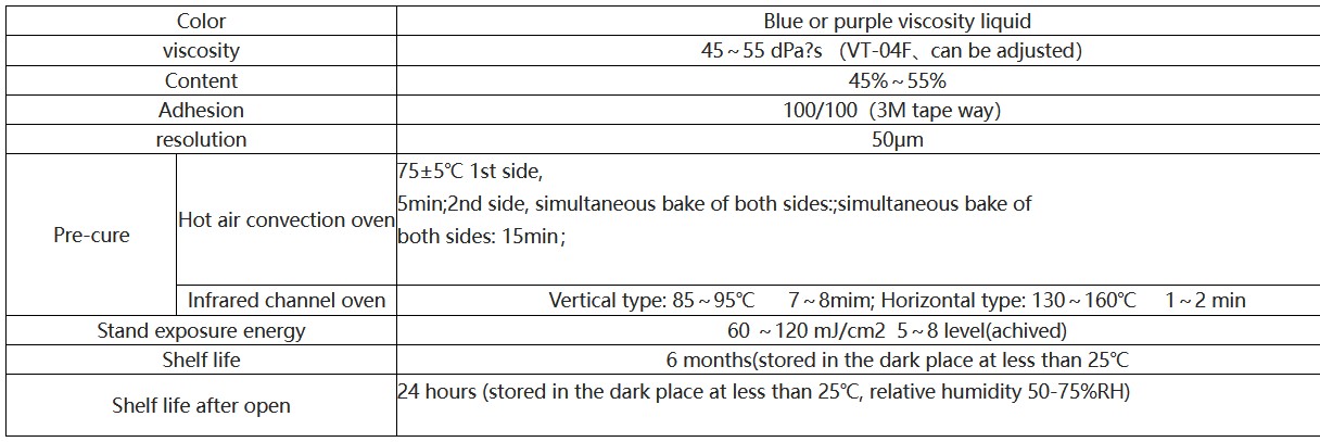
4.Parameters: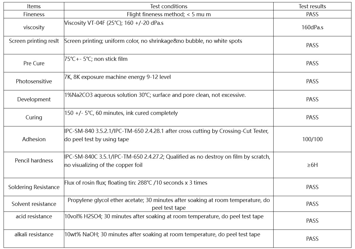
The technical parametersarefrom our internal test results. Only for your reference. We suggest you applying by setting appropriate using conditions after confirming experiment.
The technical parameters are from our internal test results. Only for your reference. We suggest you applying by setting
appropriate using conditions after confirming experiment.
1.special note:
You will found the specifications of specific model and related test reports in download center.
2.Our clients:
1、Jianding(Wuxi) Electronic Co.,LTD. 2、Shanghai Meiwei Electronic Co.LTD. 3、Yilianda Electronic Co.,Ltd. 4、Hongban(Jiangxi) Co..Ltd. 5、Yuehu circuit(Suzhou) Co.LTD
3.Application areas:
The liquidphotoimageable solder resist ink is the most important basic material in process of printing PCB production. It can protect the surface of circuit board from adheringwelding flux while solering tin for the circuit board or assembling the parts.
4.Parameters: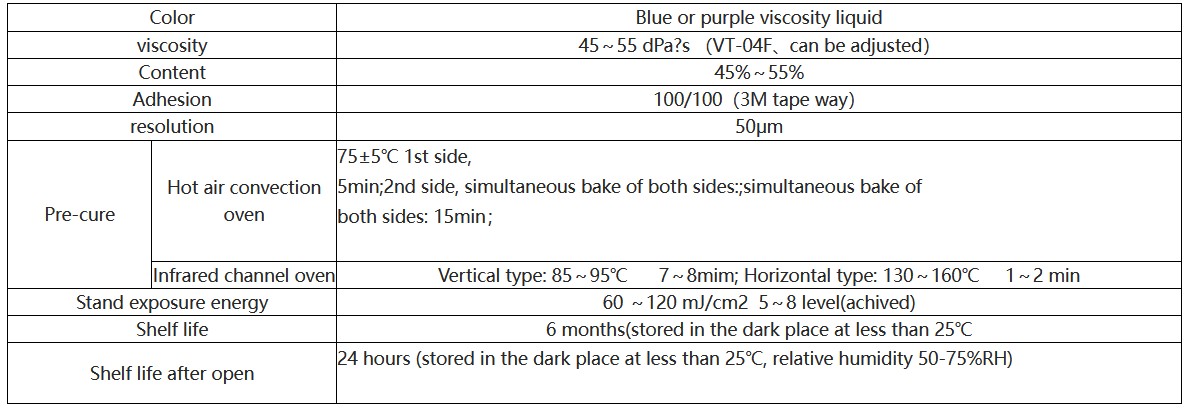
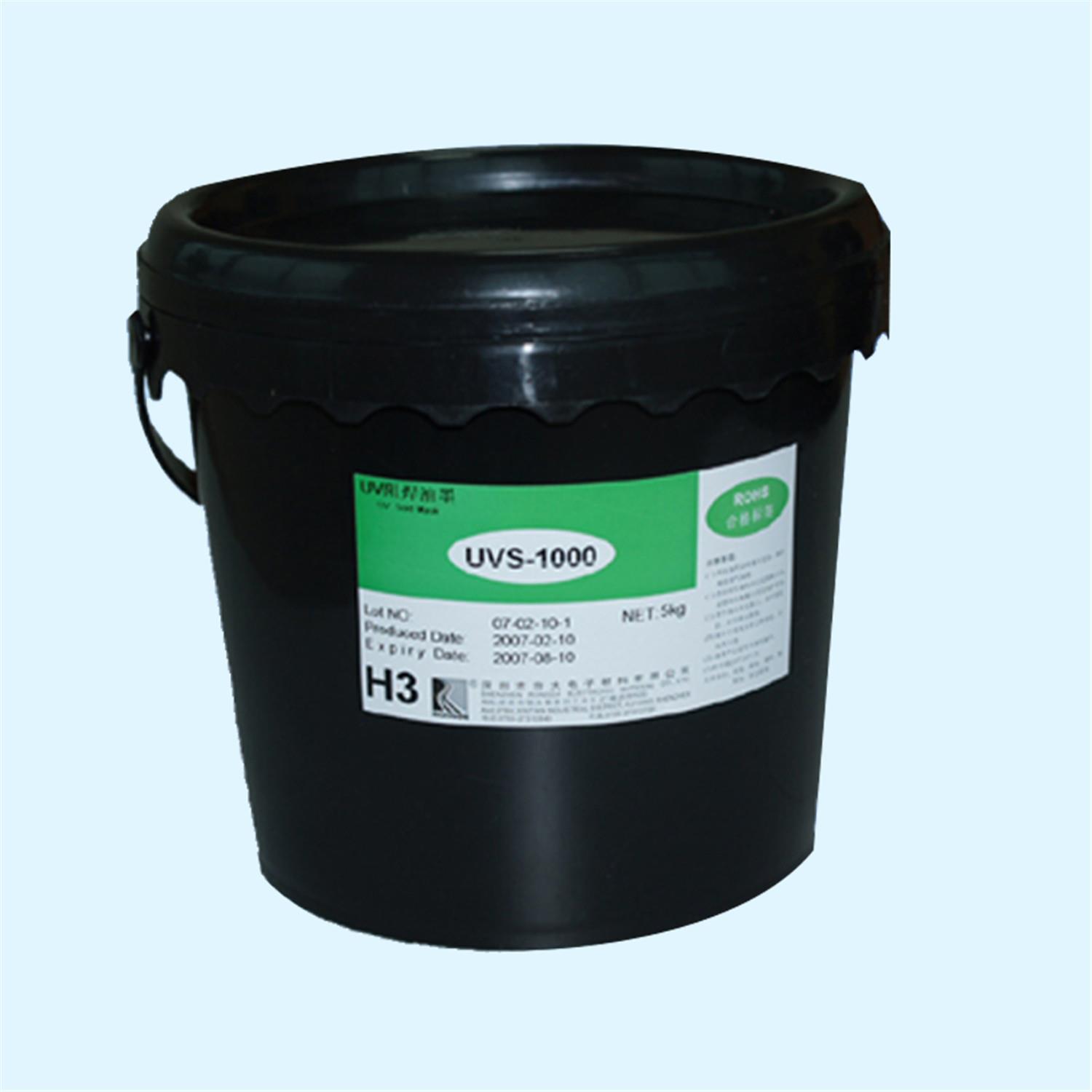
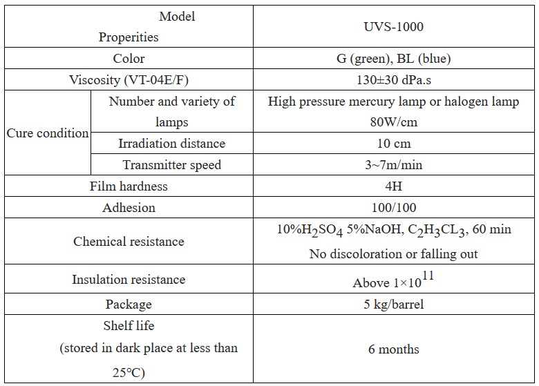
Product Specification of UVS-1000 UV Curable Solder Resist Ink
I. Introduction
UVS-1000 type solder resist ink is UV curing solder mask developed for printing circuit board. It does not contain solvent without pollution. It is characterized by fast curing, excellent adhesion after curing and excellent heat resistance and insulation. Technical parameters are showed in the following table (at room temperature condition unless otherwise noted):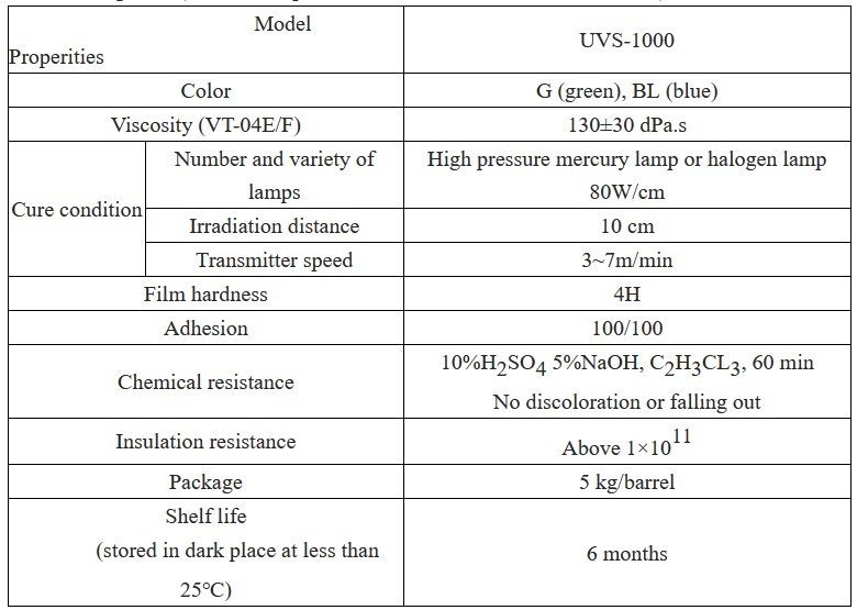
II. Process conditions
1. Oiling
Use it after mixing for 15 min thoroughly and leaving it alone for 15 min.
2. Pre-treat the substrate
3~5% sulfuric acid or hydrochloric acid for water cleaning, grinding defect for 15~20 mm, water film cracking for more than 10 sec, meshes of brushing roller 300 and 500, polish brushing current 2.5~3.0 A and drying temperature 80~120 ℃.
3. Printing
Screen 90~100T silk screen, scraping hardness 65~75, scraper angle 70~80°, inclination 20~35°, screen distance 4~6 mm, rest scraping rubber ≥15 mm, the length of scraper in one side is 10~20 mm longer than the printing graph, machine printing pressure 1.0~2.0 kgf/cm2, screen speed 50~70 HZ, printing film thickness 10~15 μm.
4. Curing
The energy of 5~8 kw mercury lamp or halogen lamp (mercury lamp) is above 1000mj/cm2, the distance to irradiate plate surface is 8~10cm and the usage time of lamp tube is controlled within 1,000 hours.
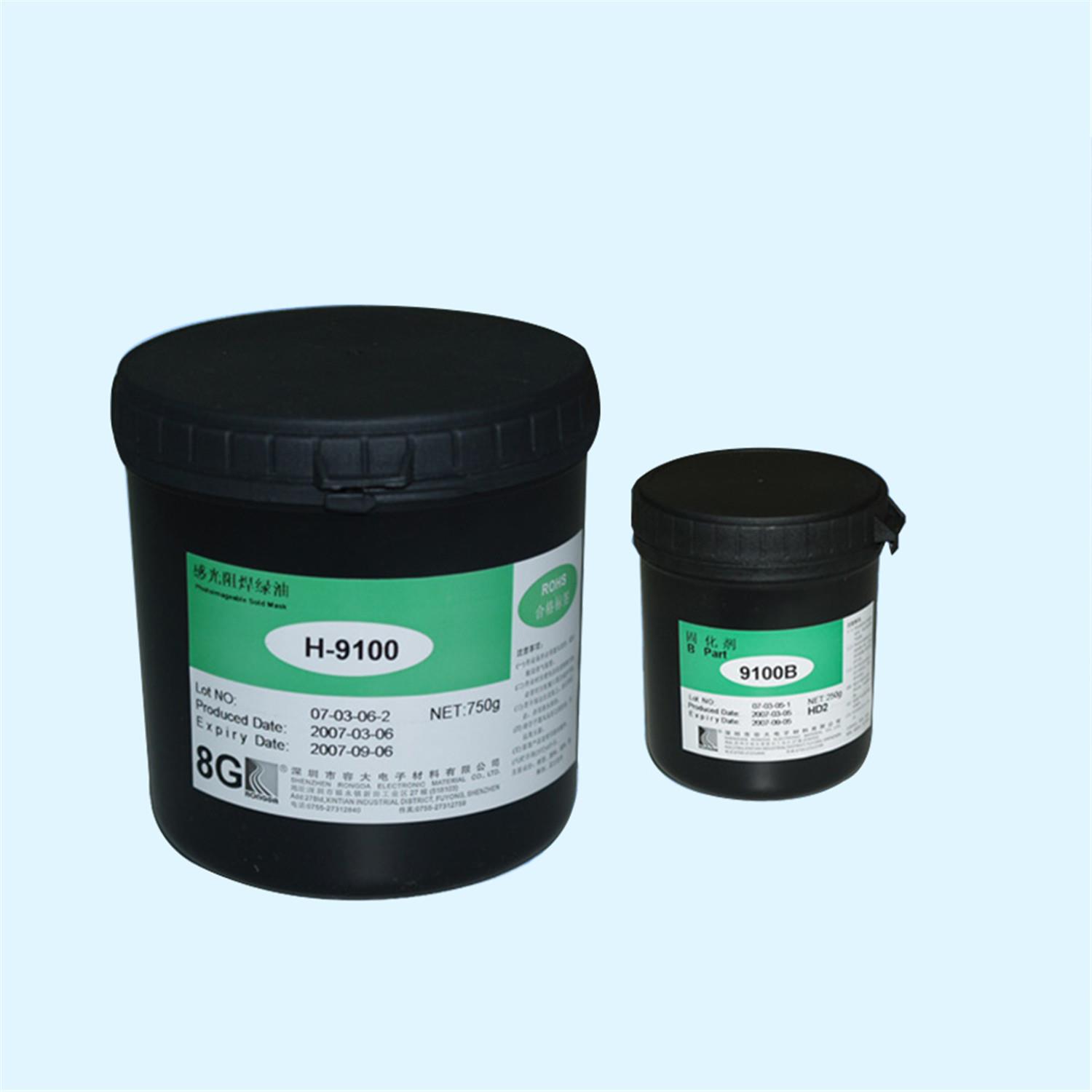
1. FEATURES:
H-8100 8WL501 is a type of bi-component dilute aqueous alkali developing liquid phptosensitive solder resist ink. it mainly has the following features:
1) Provided with fairly perfect printing behavior; capable of compactly covering the surface of the printed object;
2) Provided with excellent hardness, wear resistance, compactness cutability, chemical resistance, and heat resistance etc.;
3) Provided with excellent electrical performance;
4) It had passed the SGS Test, known as a type of environmental-friendly product.
2. Specification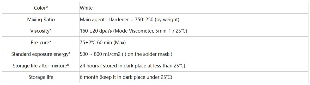
“* ”Means the situation after main agent mix up with hardener.
1、Process: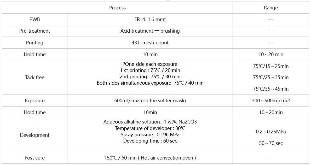
2、CHARACTERISTIC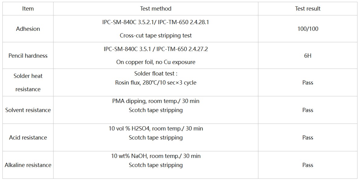
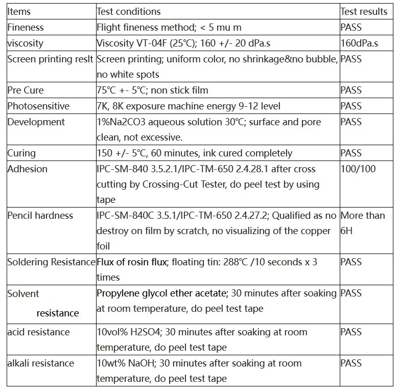
Note : The above-mentioned test data is just for reference, not to guarantee the result.
5. PRECAUTIONS
1) The product should be stored or handled at a place with temperature of 10-25℃ and relative humidity of 50-75%RH; in addition, only yellow light is allowed; do not handle the product in White electric light or sunlight (whether directly or indirectly).
2) The product should be applied in its original state; when it is necessary to adjust the viscosity, it is required to adopt diluent, and the proportion must be controlled within 3%. Please do the experiment of matching first while adopting other diluent.
3) Once the product is mixed, it should be used up within 24 hours. When opening the can, hand mix it for 1-2 min at first before machine stirring.
4) Surface treatment of bared board has a critical impact on full play of solder resist behaviors.
Before printing operation, in order to ensure that the PCB surfaces are thoroughly cleaned, dried, and the oxide layer is removed, it is advisable to treat the PCB with chemical microetch and mechanical polish-brush separately or simultaneously so as to absolutely remove the oxide, oil, fat or other pollutant on surfaces of bared boards; wash the boards with water and the
dry them adequately; avoid finger touch and carry out solder-resist printing operation as soon as possible for fear of poor adhesive power of printing ink, or degradation of solder-resist performance. Pretreatment for golden board may be soft polish-brush (polish-brush #1000 at least), citric-acid immersion or spraying. Pay special attention to the attendance of pretreatment equipment after water washing phase so that the secondary pollution of board surface can be avoided.
5) Exposure energy may vary as per different bared boards and thickness of printing ink. Please carry out test to determine the lateral
erosion grade, surface gloss and reverse-side light-sensation grade. Photometer should be set to level 9-12.
6) Adequately manage the developing solution concentration, temperature, nozzle pressure and time etc. Inadequate management may lead to poor developing performance of printing ink, lateral erosion or blister. In addition, Spray nozzle of developing machine should be regularly smoothed so as to ensure proper developing /rinsing effect in operation.
7) Developing should be within 48 hours after coating. If workshop to be warm and humid and relatively heavy, take to finish the operation within 12hours.
8) In case skin or eyes are exposed to the product, it is required to clean with soap and rinse with plenty of fresh water; do not clean with any solvent.
9) The product is inflammable, and it must not be placed or applied in a site with smoke and fire.